The Complete Turnkey PCB Assembly Process Explained Step by Step
Introduction
Modern electronics manufacturing demands speed, precision, and efficiency. Companies developing electronic products must manage complex processes that involve PCB fabrication, component sourcing, assembly, testing, and quality control. Coordinating all these stages separately can be time-consuming and expensive.
This is why many businesses now rely on turnkey PCB assembly services. A turnkey approach simplifies manufacturing by allowing a single provider to manage the complete PCB production process from start to finish.
Whether you are building consumer electronics, industrial systems, medical devices, or IoT products, understanding the turnkey PCB assembly workflow can help you improve product quality, reduce delays, and optimize production costs.
Businesses looking for reliable electronics manufacturing often choose turnkey pcb assembly services to simplify production and reduce delays. From sourcing components to final testing, everything is handled under one solution. This approach improves efficiency, ensures better quality control, and helps companies bring innovative electronic products to market faster and more cost-effectively.
This article explains the complete turnkey PCB assembly process step by step.
What Is Turnkey PCB Assembly?
Turnkey PCB assembly is a comprehensive manufacturing service where one company handles every stage of PCB production.
This usually includes:
- PCB fabrication
- Component procurement
- SMT assembly
- Through-hole assembly
- Inspection and testing
- Final packaging and shipping
Instead of managing multiple suppliers, customers work with one manufacturing partner that coordinates the entire project.
This integrated process improves efficiency, quality control, and production speed.
Step 1: Submitting Design Files and Project Requirements
The turnkey PCB assembly process begins when the customer submits all required manufacturing files.
These typically include:
- Gerber files
- Bill of Materials (BOM)
- Pick-and-place files
- Assembly drawings
- Schematic diagrams
- Testing requirements
Accurate documentation is essential because all manufacturing stages depend on this information.
Importance of Proper Documentation
Incomplete or incorrect files can lead to:
- Production delays
- Assembly errors
- Sourcing issues
- Increased costs
Most manufacturers carefully review submitted files before production begins.
Step 2: Design Review and DFM Analysis
After receiving the project files, the manufacturer performs a Design for Manufacturing (DFM) review.
This step identifies potential production problems before fabrication starts.
Common DFM Checks
Manufacturers analyze:
- Trace width and spacing
- Via sizes
- Component placement
- Solder mask clearances
- Thermal management
- Panelization efficiency
Benefits of DFM Analysis
DFM optimization helps:
- Reduce manufacturing defects
- Improve assembly yields
- Lower production costs
- Increase product reliability
Early design improvements prevent expensive rework later in the process.
Step 3: Component Procurement and BOM Verification
Once the design review is complete, the manufacturer begins sourcing components listed in the BOM.
This stage is one of the most critical parts of turnkey PCB assembly.
Component Sourcing Activities
The procurement team:
- Verifies manufacturer part numbers
- Confirms component availability
- Identifies lead times
- Sources approved alternatives if needed
- Prevents counterfeit components
Experienced turnkey providers use established supplier networks to secure reliable components quickly.
BOM Verification
Manufacturers also validate the BOM to ensure:
- Correct quantities
- Proper package types
- Compatible footprints
- Consistent part information
Accurate procurement is essential for smooth assembly operations.
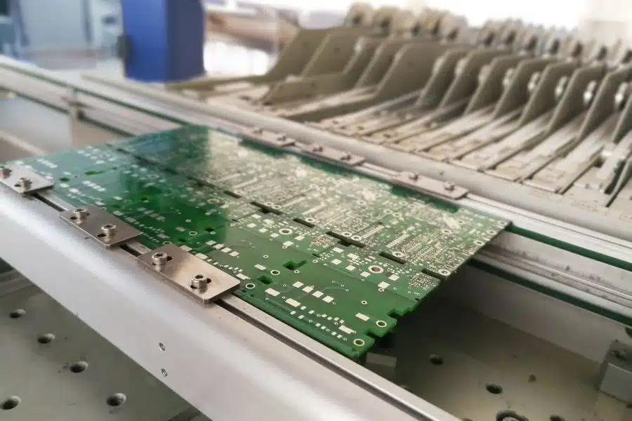
Step 4: PCB Fabrication
While components are being sourced, PCB fabrication begins.
The bare PCB is manufactured according to the Gerber files and design specifications.
PCB Fabrication Process
Typical fabrication stages include:
- Material preparation
- Inner layer imaging
- Etching
- Lamination
- Drilling
- Copper plating
- Solder mask application
- Silkscreen printing
- Surface finishing
Common Surface Finishes
Popular finishes include:
- HASL
- ENIG
- OSP
- Immersion silver
The choice depends on the application, budget, and assembly requirements.
Step 5: Incoming Quality Inspection
Before assembly begins, manufacturers inspect both the fabricated PCBs and sourced components.
PCB Inspection
Boards are checked for:
- Layer alignment
- Surface defects
- Dimensional accuracy
- Hole quality
- Electrical continuity
Component Inspection
Components are verified for:
- Correct part numbers
- Packaging integrity
- Moisture sensitivity
- Authenticity
- Quantity accuracy
This inspection stage helps prevent assembly issues caused by defective materials.
Step 6: Solder Paste Application
The PCB assembly process starts with applying solder paste to the board.
How Solder Paste Is Applied
A stainless-steel stencil is aligned over the PCB, and solder paste is deposited onto the solder pads.
The accuracy of this process is extremely important because improper solder paste application can lead to:
- Solder bridges
- Weak solder joints
- Component misalignment
Modern assembly facilities use automated stencil printers for precise application.
Step 7: SMT Component Placement
After solder paste application, automated pick-and-place machines position surface-mount components onto the PCB.
SMT Assembly Process
High-speed placement machines use programmed coordinates from the pick-and-place file to place components accurately.
These machines can install thousands of components per hour with exceptional precision.
Advantages of Automated Placement
Automated SMT assembly offers:
- High production speed
- Improved accuracy
- Reduced human error
- Consistent assembly quality
This stage is critical for modern compact electronics designs.
Step 8: Reflow Soldering
Once components are placed, the PCB enters a reflow oven.
What Happens During Reflow
The board passes through carefully controlled heating zones that melt the solder paste and create permanent electrical connections.
Temperature profiles are optimized based on:
- PCB materials
- Component sensitivity
- Solder type
Importance of Reflow Control
Improper temperature settings can cause:
- Cold solder joints
- Component damage
- Warping
- Assembly defects
Precise thermal management ensures reliable solder connections.
Step 9: Through-Hole Assembly (If Required)
Some PCBs include through-hole components that require additional assembly steps.
Common Through-Hole Components
These may include:
- Connectors
- Transformers
- Large capacitors
- Mechanical switches
Assembly Methods
Through-hole components may be installed using:
- Manual soldering
- Wave soldering
- Selective soldering
This stage is often used for components requiring strong mechanical stability.
Step 10: Cleaning and Flux Removal
After soldering, the PCB may undergo cleaning to remove residual flux and contaminants.
Why Cleaning Matters
Cleaning improves:
- Electrical performance
- Long-term reliability
- Corrosion resistance
- Cosmetic appearance
Different cleaning methods are used depending on the soldering process and product requirements.
Step 11: Inspection and Quality Control
Quality assurance is one of the most important stages in turnkey PCB assembly.
Manufacturers perform multiple inspection procedures to detect defects before shipment.
Automated Optical Inspection (AOI)
AOI systems use cameras to identify:
- Missing components
- Incorrect polarity
- Solder defects
- Alignment issues
X-Ray Inspection
X-ray systems inspect hidden solder joints, especially for:
- BGAs
- QFNs
- Multi-layer assemblies
In-Circuit Testing (ICT)
ICT verifies electrical performance and component functionality.
Functional Testing
The completed PCB is tested under real operating conditions to ensure proper performance.
Comprehensive testing significantly reduces field failures and warranty issues.
Step 12: Final Assembly and Packaging
After passing inspection, the completed PCBs move to final assembly and packaging.
Final Processes May Include
- Conformal coating
- Mechanical assembly
- Product labeling
- Firmware programming
- Protective packaging
Proper packaging protects sensitive electronics during transportation.
Step 13: Shipping and Delivery
The final stage is shipping the completed PCB assemblies to the customer.
Professional turnkey PCB assembly providers often offer:
- Global shipping
- Inventory management
- Drop shipping
- Production scheduling support
Reliable logistics help maintain efficient supply chain operations.
Advantages of the Turnkey PCB Assembly Process
The turnkey model offers several important benefits.
Faster Production
Integrated workflows reduce delays and improve manufacturing efficiency.
Simplified Communication
Customers work with one supplier instead of multiple vendors.
Better Quality Control
Centralized production improves consistency and defect management.
Reduced Costs
Bulk sourcing and streamlined logistics lower overall manufacturing expenses.
Improved Scalability
Turnkey providers support everything from prototypes to mass production.
Industries Using Turnkey PCB Assembly
Turnkey PCB assembly supports many industries, including:
- Consumer electronics
- Medical devices
- Automotive electronics
- Telecommunications
- Aerospace systems
- Industrial automation
- IoT technology
As electronics become more advanced, turnkey manufacturing continues to grow in importance.
Conclusion
The turnkey PCB assembly process combines fabrication, sourcing, assembly, testing, and logistics into one streamlined manufacturing solution. By managing the entire workflow under a single provider, companies can reduce complexity, improve quality, accelerate production, and lower operational costs.
Understanding each stage of the turnkey PCB assembly process helps businesses make better manufacturing decisions and avoid common production challenges.
As demand for high-quality electronics continues to increase, turnkey PCB assembly remains one of the most efficient and reliable manufacturing solutions available today.